Technology
Physical Design
Advanced Process Design
SEMIFIVE has accumulated extensive experience in advanced process technologies. Being the first Samsung Foundry’s DSP to design an SoC based on the the foundry’s 5nm process for their customer, SEMIFIVE has been enabling its customers to take advantages from leading FinFET process nodes such as Samsung Foundry’s 5nm, 8nm, 14nm and more. Through such experience, we work with our customers to explore design options and develop the best solution to meet each of their specific application’s requirements.

Design Expertise in Various Applications
Purpose-built custom chips create value by focusing on specific applications. In other words, the value can be maximized when every aspect of design is tailored and optimized for the target application. This is why design experience across various applications is essential in SoC designs today. Physical Engineering team members at SEMIFIVE have wide experience designs covering AI, LTE/5G, Vision/Camera, Digital TV, Mobile, AIoT and Automotive end markets. Meet the exact experience for the success of your next chip with SEMIFIVE.
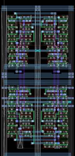
Our Physical Design Capabilities
- Place and Route in advanced FinFET nodes (14nm/8nm/5nm and more)
- Tapeout experiences in Samsung Foundry 5nm
- Experienced Complex Power Domains with UPF
- Parasitic Extraction with StarRC
- Physical Verification Signoff with ICV and Calibre
- IR/EM/Jitter signoff with Redhawk and Redhawk-SC
- Timing ECO and signoff with PrimeTime
- Physical Synthesis/SCAN/BIST
- Low power implementation and signoff
- Full-Chip SoC tapeout
Examples of Design Projects
Get More Info
"*" indicates required fields